Image Processing Reference
In-Depth Information
Copy
Original
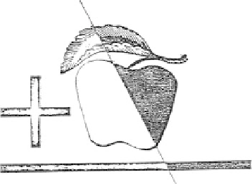
FIGURE 10.13
Example of the gray-scale image without a biased development electrode.
Copy
Original
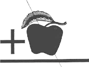
FIGURE 10.14
Example of the gray-scale image with a biased development electrode.
|
V
h
|
V
dev
V
bias
V
clean
|
V
L
|
FIGURE 10.15
Development and cleaning voltages in a CAD system.
discharged region, then the development and cleaning voltages can be written as
(Figure 10.15)
V
dev
¼
V
h
V
bias
V
clean
¼
V
bias
V
L
(
10
:
28
)
For DAD, which is more commonly used than CAD, only the discharged areas of the
photoconductor will attract toner from the development zone. Other negatively


Search WWH ::

Custom Search