Information Technology Reference
In-Depth Information
Barrier Height
A
B
C
D
1234 56 7 89 011
12
13
14
Clock Cycle
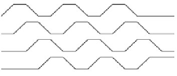
Fig. 10. The four clock signals used to drive the device shown in Fig.
9
. Again, note the highly
regular nature of these clock signals, which repeat the pattern shown in Fig.
5
three times each.
Polarizaion
1
A
B
C
in
X1
X2
X3
0
1
1
1
1
0
1
1
1
1
0
M1
1
1
0
M2
1
1
0
0
M3
Sum
C
out
1
0
1
0
0
0
1
1
1
1
123 456 7 89 011
12
13
14
Clock Cycle
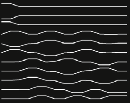
Fig. 11. The states of labeled cells throughout the operation of the device in Fig.
9
when
A = 1, B = 0, and C
in
= 1. These inputs are only applied during the first clock cycle, and their
contents are propagated through the device at different speeds so that they arrive at M1-M4 at
the same time. The correct output, shown at the bottom right corner of the figure, first appears
during the 12
th
clock cycle. These results are the outcome of simulating the device in Fig.
9
using the clock signals in Fig.
10
for 14 clock cycles.
Each time one of the input signals reaches another vertical wire, it is allowed to
drive the entire length of that wire, since the input signal that originally drove it in
clock cycle #1 has been removed. Whereas in the two-input XOR gate, only one
vertical wire had to be traversed, now the leftmost signal must cross two vertical
wires. This is not a problem, but it does require four more clock cycles for the signal
to progress through the three-input SDN. In this way, the SDN for this device delivers
12 distributed copies of its three inputs during clock cycle #10 (as compared to clock
cycle #6 for the two-input device). The combinational logic gates then require two


Search WWH ::

Custom Search