Information Technology Reference
In-Depth Information
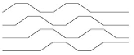
Barrier Height
A
B
C
D
1
2
3
4
5
6
7
8
9
10
Clock Cycle
Fig. 5. The clock signals applied to the SDN-based XOR gate shown in Fig.
4
. These signals
are highly regular, repeating the same pattern. The color-coded cells to the left of the y-axis
labels correspond to the coloring in Fig.
4
(b).
This will be handled by the clock signals shown in Fig.
5
and by carefully assigning
individual cells to the corresponding clock signals.
During clock cycle #2, the X input signal propagates one cell to the right (into
the cell colored green in the color version of Fig.
4
(b)). In clock cycle #3, it moves
one more cell to the right into the yellow cell, and in clock cycle #4, it moves one
more cell to the right into the red cell, which is also labeled cell #1 in Fig.
4
(b). Clock
cycle #5 is the key to this device's operation. Since the inputs X and Y were only
applied during the first clock cycle and were then removed, the right-hand vertical
wire is now available to be driven by cell #1. Through the interaction between cell #1
and cell #2, the entire right-hand vertical wire is driven to contain the value of input X
during clock cycle #5. Note that this signal was originally contained in the left-hand
vertical wire during clock cycle #1. In clock cycle #6, the signal is available along the
entire length of the right-hand vertical wire, so copies can be made at any needed
location, such as at cell #3.
At this point, the signals have been fully distributed, and no additional wire
crossings will be needed. However, input Y, which was originally on the right-hand
vertical wire, will arrive at its destination five clock cycles before input X unless we
take corrective action. This problem is solved by carefully assigning the cells on each
horizontal wire to clocking regions of varying widths. The wires containing signal Y
take very small steps, with each clock signal assigned to just one or two cells.
By contrast, signal X moves very quickly from cell #3 to the AND gates because those
entire lines all belong to the same clock signal. In this way, the signals corresponding
to X and Y each arrive at the AND gates during clock cycle #6, the AND calculations
are completed during clock cycle #7, and the OR calculations yield the final output
during clock cycle #8.
The contents of each of the labeled cells in Fig.
4
(b) for each clock cycle can be
seen in Fig.
6
, and Fig.
7
shows a series of snapshots of the device at key phases of its
operation.
Although this device requires eight clock cycles to complete the XOR function,
only six of these are used by the SDN. The remaining two clock cycles are used to
implement the (relatively simple) combinational logic. The device was simulated for
all four possible combinations of the two inputs, and each was found to yield the
correct result.


Search WWH ::

Custom Search