Information Technology Reference
In-Depth Information
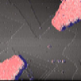
QCA circuitry. Recently, our reevaluation of non-idealities inherent to the
scanned probe fabrication process and in the character of the scanned probe
tip itself have led to a large improvement. Yields of a tiny fraction of 1 % have
jumped to 80 %. The various refinements will not be discussed here but the
results can be seen in Fig.
19
. A 16 atom, 4 QCA cell is shown with one atom
out of place. Further study has uncovered the dominant reasons for this remnant
fabrication error and it is anticipated that as new fabrication tools come on line
in the year ahead that improved yields will result. As a test of larger pattern
fabrication capacity, and despite the errors still produced, two well studied QCA
circuits from the literature [
39
] were made. We see good overall pattern fidelity
and a clear demonstration that we have broken free of the 4 atom limit of a
few years ago and may soon be able to make 100 atom structures with excel-
lent fidelity. The circuits in Fig.
19
required about 1 min to fabricate and were
automatically made by computer upon input of pattern required.
Substrate defect elimination, automatic fabrication error correction,
as-needed on the fly rerouting and circuit redundancy strategies are all parts of
the plan to achieve functional devices within the next several years. Numerous
18
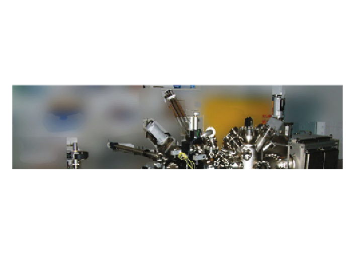
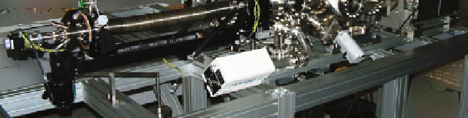
Fig. 18.
A multi-probe STM has been developed to allow nano-scale electrical charac-
terization that had previously been beyond reach. The instrument has three indepen-
dently scannable tips, watched over by a scanning electron microscope. Each tip can
be deployed as a scanned probe for imaging or touched down as a current source or
as a voltage probe. Nanoscale potentiometry and transport measurements have been
made with the instrument.


Search WWH ::

Custom Search