Information Technology Reference
In-Depth Information
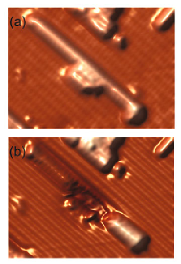
Fig. 14.
STM images of single-triple CF
3
-styrene/OCH
3
-styrene heterostructure.
(a) V
s
=2V.(b)V
s
=
−
2V. Single OCH
3
-styrene and CF
3
-styrene lines image above
H-Si surface, while triple CF
3
-styrene chains image below H-Si surface.
is occupation. The wider spaced molecule tolerates a larger negative charge com-
pared to the tightly spaced molecule. The latter has one electron. The widely
spaced molecule has two electrons and those repel one another, leaving the cen-
tral atom approximately neutral on average, and brighter in appearance. The
complex arrangement labeled (d) uses both tunnel coupled atoms and perturb-
ing atoms on the periphery to locally change the character of individual atoms
and thereby the properties of whole ensemble.
Figure
13
c shows a linear chain of ASiQDs. Such a structure will delocalize
charge and allow biasing wires to be fabricated where needed. Such wires will
bridge between relatively large lithographically created structures and the atom
scale, allowing intimate input. It is a compelling feature of the ASiQD approach
to circuit fabrication that high density ensembles enable passive components
such as wires to be made while somewhat more widely spaced structures allow
for the creation of the active elements in a circuit.
Molecules of designed optical properties can be made. This has been touched
upon in a recent charge qubit characterization discussion [
24
]. More complex
control is however possible. Not only the absorption energy, but the mode of
adsorption can be pre-defined, whether electric dipolar, magnetic dipolar, or
complex multipolar. The particular polarization dependence of absorption can
Search WWH ::

Custom Search