Information Technology Reference
In-Depth Information
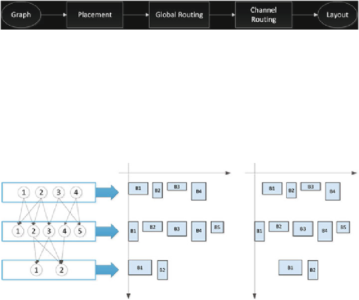
Fig. 13.
Physical Mapping flow diagram. The circuit layout is generated starting from
its graph following several optimization steps.
Placement.
During the placement stage each node of the graph is mapped into
its logic gate. As shown in Fig.
14
, nodes are placed row by row starting from
the top of the graph without any optimization. Thus, blocks are aligned with a
minimum spacing equal to one equivalent magnet height.
Fig. 14.
Center
: seed row placement for maximum with evaluation;
Right
: barycentered
placement
This technique is used to evaluate the maximum width of the circuit, i.e the
width of the largest row. At this point, a barycenter alignment is performed to
shift placed blocks in order to reduce the overall wire length.
Global Routing.
The final position of each gate is obtained with a fine shift
performed during the global routing phase. The idea is to maximize the circuit
compaction, therefore reducing the length of interconnection wires. Figure
15
shows the flow diagram of the global routing phase.
The implemented procedure is composed by the following main steps itera-
tively applied to each couple of rows:
- Logic gates of row
i
are shifted.
- Wires among row
i
and row
i+1
are routed.
- Interconnection area is evaluated.
Search WWH ::

Custom Search