Information Technology Reference
In-Depth Information
they see from one side magnets that are in the HOLD state (no magnetic field
applied). Magnets in the HOLD state can assume a value of logic '0' and '1' so
they are seen as an input by magnets that are switching. At the same magnets
near the other side of the switching zone are in the RESET state (magnetic
field is applied) and therefore they have no influence on the switching ones.
Figure
3
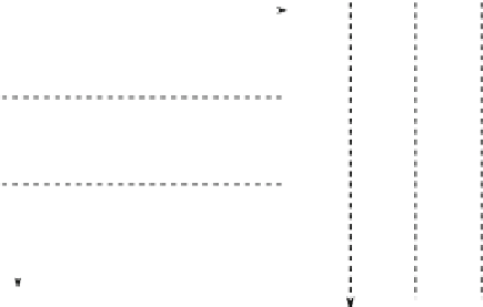
(B) shows the circuit time evolution when a multiphase clock system is
used.
CLOCK
CLOCK
CLOCK
Space
SIGNAL 2
SIGNAL 3
SIGNAL 1
I/Imax
CLOCK
CLOCK
CLOCK
PHASE1 PHASE2 PHASE3
TIME
STEP 1
SWITCH
RESET
HOLD
TIME
STEP 2
HOLD
SWITCH
RESET
TIME
STEP 3
RESET
HOLD
SWITCH
Time
Time
Time
(A)
(B)
Time
Fig. 3.
3-phase clock. Circuits are divided in areas, called clock zones, made by a
limited number of magnets. (A) Three clock signals with a phase difference of 120
◦
are selectively applied to clock zones. (B) When magnets of a clock zone are in the
SWITCH state, magnets on the left are in the HOLD state and act like an input, while
magnets on the right are in the RESET state and have no influence on the switching
magnets.
To design circuits, clock zones must be arranged following a proper layout.
Moreover the layout must take into account the constraints related to the tech-
nological fabrication of the clock generation network. For example the magnetic
field is normally generated by a current flowing through a wire placed under the
magnets plane [
25
] (Fig.
4
(A)). With this clock mechanism the clock zones lay-
out is made by parallel stripes (Fig.
4
(B)). Each stripe corresponds to one of the
clock wires used to generate the various clock signals [
13
]. While this layout was
developed for the magnetic field clock, and other clock systems can have different
layouts, it has the advantage to synchronize signals propagation. Thanks to the
multiphase clock the circuit is intrinsically pipelined, that means every group of
3 consecutive clock zones has a delay of 1 clock cycle. As a consequence, if the
length of input wires of a logic gate is not the same, signals will have different
propagation delay and propagation errors will occur. This problem is called “lay-
out=timing” [
26
,
27
]. With the clock zones layout shown in Fig.
4
(B) the length
of every input wire of any gate inside the circuit is always equalized, solving
therefore the “layout=timing” problem. For this reason this clock zones layout
is chosen as a reference regardless to the clock mechanism used.


Search WWH ::

Custom Search