Graphics Reference
In-Depth Information
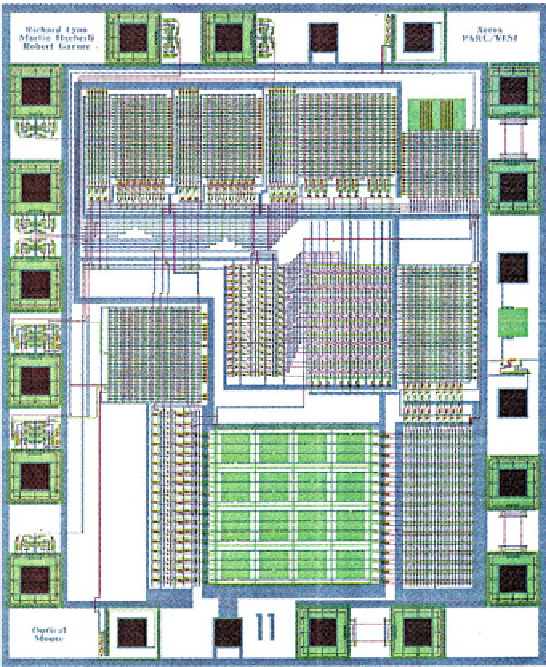
Fig. 1.18
The layout of the second-generation Xerox optical mouse chip, completed by Martin
Haeberli and Robert Garner after I left Xerox, incorporated more regular arrays outside the more
compact photodiode array, which was a more efficient use of space. This new version also incor-
porated testability features; a second connection to each photodiode allowed it be discharged elec-
trically, simulating light falling on it
photodiodes, in a way that leads to simple and elegant semi-digital designs that could
be prototyped on a by-then-standard MOS fabrication service based on Conway's
simplified design rules [
25
].
The 1981 patent filing (see Fig.
1.20
) did not go very meta; it was divided into
an imaging array with predetermined stable output states (… each of said cells
coupled with several of said neighboring cells in said array to alter the output of said
neighboring cells resulting in the recognition of said intermediary pattern as being
one of a limited plurality of predetermined such patterns …), and a cursor control
device using it.
In 1982, I presented the optical mouse design at the
Physics of Computation
class
that Mead, Hopfield, and Feynmann were jointly running at Caltech. This connection
led to my joining the Caltech faculty as visiting associate for 13 years, where I helped