Information Technology Reference
In-Depth Information
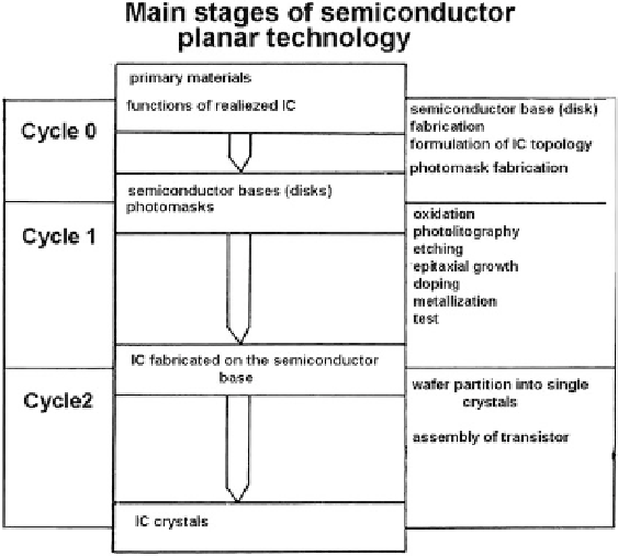
Fig. 2.13 Main stages of semiconductor planar technology
It is thus an approach utilizing the top-down principle. The essence of this
principle, characteristic, for example, for the production of macroscopic parts of
mechanical devices, is easy to illustrate using the manufacturing process of com-
plex metal parts as an example. The process starts with the part blank which is
successively subjected to turning, machining, boring required holes, cutting thread,
etc. As a result of these successive operations, the part blank is turned into the final
detail specified in the drawing. The planar technology uses various operations to
create a layer of the required material. Insulating layers of silicon oxide are grown
by controlled oxidation of the silicon substrate surface. Alternatively spraying,
deposition from the liquid phase, etc., can be used to form the films as well. The
main tool for creating individual elements of the chip is photolithography
(Fig.
2.14
). During the photolithographic process, photoresist is applied to a film
of the material from which the elements of the integrated circuit are formed.
Photoresist is a photosensitive compound which either decomposes upon light
exposure (positive photoresist) or polymerizes, forming a solid film (negative
photoresist). Photoresist is exposed through a photomask whose black and white
pattern determines the shape and the location of details to be formed on the surface
of the circuit. The photoresist film is subsequently “developed,” that is, treated with
solvent, which removes film areas unconverted by light. As a result, the photoresist
film is transformed into a stable mask. Through its windows the material can be
affected, e.g., by oxidation, doping, etc.