Information Technology Reference
In-Depth Information
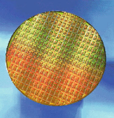
Fig. 2.12 Silicon wafer at
the stage of producing
integrated circuits
Today the semiconductor planar technology plays a central role in the produc-
tion of electronic circuits (chips) that are used in a large number of devices—
computers, control, and communication devices. It relies on a wide variety of
specific processes that differ in their physicochemical nature and the instrumen-
tation used. Typical for semiconductor technology are the extreme requirements
imposed on the purity of raw materials, handling medium (water, auxiliary mate-
rials), and the atmosphere of the production facilities. In chemical practice, both in
research and production, a substance is considered pure if the concentration of
impurities does not exceed 0.001 %. The number of atoms in 1 cm
3
of the semi-
conductor is 10
22
. Doping a semiconductor usually involves introducing 10
16
-10
19
dopant atoms per 1 cm
3
, i.e., 0.0001-0.1 %. This means that the concentration of
harmful impurities in silicon, which may affect its semiconducting properties, must
be below 0.00001 %.
The planar technology is characterized by a number of other important features.
However, since the main focus of this topic is on the interaction and mutual
influence of the computer technology and nanotechnology, we will confine consi-
deration to the most important problem in this context—the lithographic process
and the limits it imposes on miniaturization of electronic circuits.
2.3 Planar Semiconductor Technology:
Universal Acceptance and Limitations
Planar technology (see Fig.
2.13
) involves successive application on the surface of
the silicon substrate of thin layers of material which serves to form the individual
elements of the scheme, with subsequent processing of this layer.