Information Technology Reference
In-Depth Information
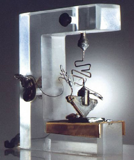
Fig. 2.9 First Bardeen and Brattain transistor
disappeared as a result of recombination will be replaced by new ones due to
diffusion through the junction, leading to constant direct current. Similarly, if the
field is applied in the reverse direction (reverse bias), the current through the
junction will be vanishingly small (Fig.
2.9
). Thus, the p-n transition behaves as
a semiconductor diode.
All these properties of semiconductor materials and p-n and n-p junctions were
used to create a unique semiconductor device—the transistor—which changed the
face of computing devices. Today this name applies to a large group of semi-
conductor switching devices with two stable states.
In 1946 William Shockley, Walter Brattain, and John Bardeen at Bell Labo-
ratories in New Jersey (AT&T Bell Labs) started to work on a semiconductor
device—the transistor. In 1947 Bardeen and Brattain demonstrated the first imple-
mentation of a transistor on the basis of a germanium crystal with p- and n-zones,
with metallic wires connected to the junction (Fig.
2.9
, reference 6 in Chapter 2).
Based on their work Shockley analyzed the physics of the device and a few months
later proposed a fully planar semiconductor transistor. In 1956 Shockley, Bardeen,
and Brattain received a Nobel Prize for this work. In his Nobel lecture John Bardeen
said: “I knew the transistor was important, but I never foresaw the revolution in
electronics it would bring.”