Information Technology Reference
In-Depth Information
(b)
(a)
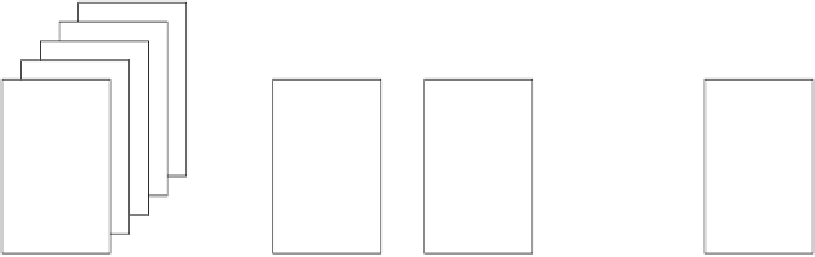
Figure 12.5
Two simulations of a
T
-step VLSI chip computation by a planar circuit.
the number of crossings does not exceed
r
2
C
Ω
(
f
)
2
/
2 because there are at most
2
ways of
forming pairs drawn from a set of size
q
and
q
=
rC
Ω
(
f
)
. Combining this with the number
of inputs and gates, we have the desired upper bound.
In Section
12.7
we show that
f
(
n
)
cyclic
nearly meets the upper bound of Lemma
12.6.1
.That
is, the planar circuit size of this function is nearly quadratic in its standard circuit size.
12.6.2 Computational Inequalities
We now show that every VLSI chip computation can be simulated by planar circuits of size
O
(
AT
2
)
and
O
(
A
2
T
)
. The simulation is patterned on the simulations of Chapter
3
;thatis,
the loop that constitutes the computation by the chip with memory is unwound to create a
planar circuit. Instead of passing the outputs of the next-state/output circuit to binary memory
cells they are passed to another copy of the circuit.
Figure
12.5
showstwosimulationsofa
T
-step VLSI chip computation by a planar circuit.
The first is obtained by placing
T
copies of the chip one above the other and supplying the
state output of one copy to the state input of the next copy. The second is simulated by placing
T
copies of the chip side by side and running wires from the state output of one chip to the
state input of the next. We convert each of these memoryless circuits to planar circuits and
bound the number of inputs, crossings and gates they contain. Recall that we assume that
wires are rectilinear; that is, they run only horizontally and vertically.
Since the number of wire layers on a single chip is bounded, it does not hurt to assume
that the centerlines of parallel wires on different planes are displaced slightly. (It is bad practice
to overlap wires because one wire can induce currents in the other.) Now make the width of
wires and the area of gates infinitesimal. (Wires are shrunk to their centerline.) As shown in
Fig.
12.6
(a), each two-input gate is replaced by an infinitesimal vertex connected by a straight-
line to its output and the two connections from its inputs are made by wires that contain bends
(two wires touch). This converts a single chip to a planar graph with wires that touch or cross.
(See Fig.
12.6
(b) and (c)).
We now bound
n
w
,thenumberofwires,and
n
g
, the number of gates on a chip of area
A
. Since each wire has width
λ
and length at least
λ
and each gate occupies area
λ
2
,
n
w
and


Search WWH ::

Custom Search