Environmental Engineering Reference
In-Depth Information
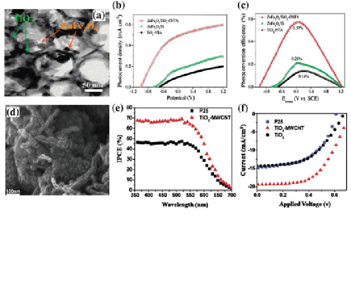
Fig. 16 SEM images of ZnFe
2
O
4
/TiO
2
nanotubes (a) and TiO
2
MWCNT nanocomposite (d).
b Variation of the photocurrent density versus bias potential (versus SCE) and c Photoconversion
efficiency as a function of the applied potential (versus SCE) based on (a). IPCE curves (e) and
current-voltage characteristics (f) of DSSCs based on TiO
2
MWCNT nanocomposite (c).
(Reprinted with permission from Ref. a-c [
365
], d-f [
366
]. Copyright American Chemical
Society)
Several synthetic strategies have been designed to fabricate graphene-TiO
2
photocatalysts. In the first method, well-defined TiO
2
structures are deposited on
the surface of graphene oxide (GO) under vigorous stirring or ultrasonic agitation
[
368
-
370
]. The site-specific oxygenated groups on GO favor a uniform distribu-
tion of TiO
2
across the surface. Graphene-TiO
2
photocatalysts are obtained after
the reduction of GO in the composite [
371
,
372
]. Yang et al. packed TiO
2
and
graphene nanosheets into a 2D unit (TiO
2
/graphene) that is structurally similar to a
thylakoid in the chloroplast of photosynthetic plants. In this 2D unit, TiO
2
per-
forms as a photo-electric conversion center to absorb light and excite the electrons,
while graphene is like the cytochrome b6f complex capturing electrons and
transporting them out of the circuit. Such a novel structure was formed by stacking
TiO
2
nanosheets and GO nanosheets using a layer-by-layer (LBL) assembly
technique in the presence of charged poly(diallyldimethylammonium chloride)
(PDDA) which supplied the counter-ions. GO was reduced to graphene by
hydrazine and annealed under argon flow at 400 C and the PDDA was then
removed by calcining at 450 C in air. The graphene-TiO
2
stacking film can
produce an anodic current 20 times larger than pure TiO
2
stacking films. Inter-
estingly, the current further increased with thicker films [
373
]. Another significant
example, graphene-wrapped anatase TiO
2
nanoparticles (Fig.
17
a) with a signifi-
cant reduction in the band gap (2.80 eV, Fig.
17
b) were prepared by wrapping
Search WWH ::

Custom Search