Environmental Engineering Reference
In-Depth Information
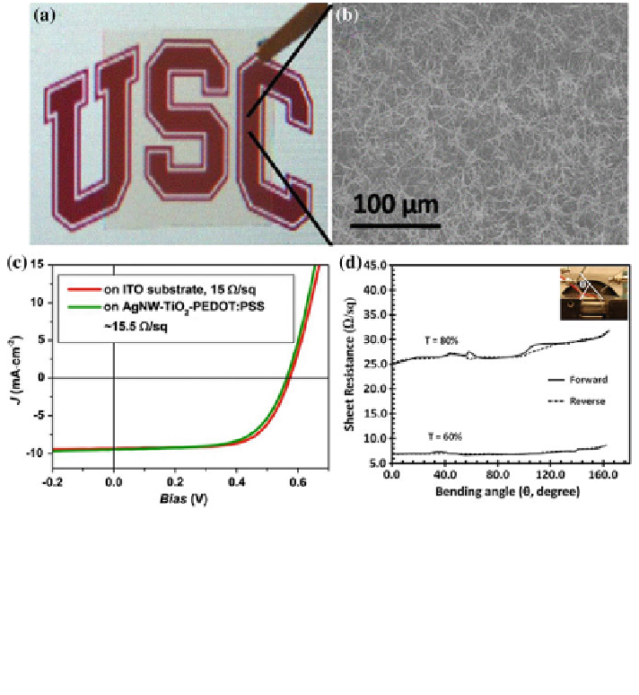
Fig. 12 a Photograph of a silver nanowire film deposited on a *2 9 2 cm PET substrate with T
80 % and R
sh
25 X!
-1
; b SEM image of the percolating nanowire distribution of the sample
shown in a; c IV curve of P3HT:PCBM cells on ITO or AgNW/TiO
2
/PEDOT:PSS substrates; d A
plot of R
sh
versus bending angle of two Ag nanowire films deposited on PET with transmittance
values of 60 and 80 %. The solid lines represent the change in sheet resistance during bending
and the dotted lines represent the change in sheet resistance during unbending. TheAg nanowire
film remains conductive even under severe bending. (a, b, and d) reprinted from Ref. [
35
] IOP
Publishing, 2013. Reproduced with permission from IOP Publishing. All rights reserved. c
2013 Amercian Chemical Society. Reprinted, with permission from Ref. [
33
]
Research on metal nanowires is very recent. So far, studies on NW films have
affirmed its applicability as an effective replacement to ITO. Currently, research on
metal nanowires is slowly gearing toward finding large-scale compatible tech-
niques. In early reports, metal NW films were processed by drop casting a sus-
pension of surfactant-assisted dispersed AgNW, followed by annealing [
27
,
30
].
Such a processing method is not scalable and cannot generate uniform films over
large area. As such, these films were less than a cm
2
of area. Spray-coating is a
scalable technique that has been recently employed in the preparation of large-area
AgNW transparent substrates [
36
,
37
]. A composite AgNW and PEDOT:PSS, both
spray coated consecutively have demonstrated low roughness and a R
sh
of 10 X
!
-1
with a mean optical transmittance of 85 % without any annealing steps [
37
].
Search WWH ::

Custom Search