Environmental Engineering Reference
In-Depth Information
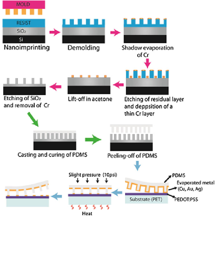
Fig. 9 Schematic illustration of the fabrication procedure of the narrow line width mold and
subsequent steps in the preparation of metal nanogrids. Color of the arrows indicates three stages
involved: NIL stage in preperation of mold (magenta), preparation of PDMS stamp (green), and
metal transfer to the final substrate (blue). 2013. John Wiley and Sons and IEEE. Adapted, with
permission from Refs. [
18
,
20
,
26
]
A number of factors influence the R
sh
of random network of NWs: wire length,
wire resistance, wire-to-wire contact (junction) resistance, and wire density. At
very low density, the effect of the junction resistance is more pronounced. This is
because of significantly greater number of parallel NW connections present at
higher densities, hence the lowest resistance determines the overall resistance of
the film [
27
]. Higher densities, however, require a trade-off with optical trans-
parency. Nevertheless, a random network of silver nanowires scatters a significant
amount of transmitted light which can result in improved photocurrent generation
when incorporated in solar cells. Reports suggest that as much of 20 % of trans-
mitted light is scattered at [10 in Ag nanowire network [
27
].
Search WWH ::

Custom Search