Information Technology Reference
In-Depth Information
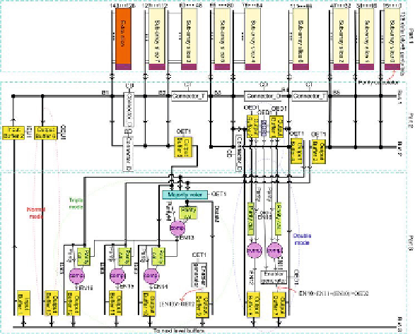
Fig. 8.
Address Decoder and Sub-Array in Flexicache
For writing the selected cache line in SVM, signal IEU1 is high and activates input
buffers IB1 and IB2 and data can transfer to the selected cache-line via Bus4 and
Bus1; and similarly for reading the selected line, signal OEU1 is high and output
buffers OB6 and OB13 are active and data is transferred from Bus1 to Bus3. Bus3
(Bus4) is connected to output data drivers (input data drivers) which are located close
to each sub-array. At each access time, the enabler signals (CDE and CTE) are high
and activate connector buffers, CD1, CD2, CD3, CD4, CT1 and CT2 and connect
nodes B1, B2, B3, B4 and B5 to each other (Each connector buffer contains two series
inverters with enablers). Similar to many typical L1 caches error protection is based
on bit-parity calculation in order to achieve high performance. We divide each cache-
line into 8 partitions each contains 16 bits where each interleaved parity protects one
partition. At each reading time parity bit calculated and compared with the original
parity bit.
For writing in DVM, signal IEU1 is high and data is transferred from Bus4 to Bus1
via IB1 and IB2 and is written to two selected lines at the same time. Parity calculator
circuits generate parity bits and write them in parity bit cells as well. For reading the
two selected lines, signals CTE is high and CDE is low, connector buffers, CD1, CD2,
CD3 and CD4 disconnect B1 with B2 and also B3 with B4 while connector buffers, CT1
and CT2 connect B2 with B3 and also B4 with B5. With this method, Bus1 is divided
into two parts; sub-array slices 0,1,2,6 are connected to the first part and sub-array
slices 3, 4, 5, 7 are connected to the second part. Signal OED1 is high; output buffers
OB1 and OB2 transfer two selected data to the XOR circuit to check the cell contents
are identical. Signal EN10 activates two parity calculator circuits to calculate parity
bits of selected lines. Then the result of these parity calculator circuits are compared
with the original parity bits of each selected-lines. These two comparators generate two