Information Technology Reference
In-Depth Information
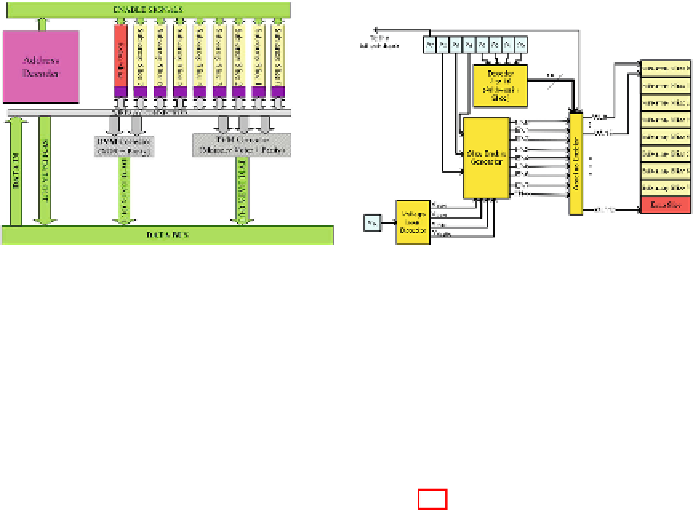
(a)
Details of the Subarray
(b)
Address Decoder
Fig. 3.
The figure presents the basic components of Flexicache such as buses, decoder
and Address Decoder
sub-array to eight equal slices (i.e sub-array slice) each containing 16 lines with
the individual precharged circuit, the write circuit, the sense amplifier circuit
and input and output buffers. Also, it extends each sub-array with an extra
slice (i.e. to make it divisible by 3). In Figure 2b, we show the layouts of one
sub-bank [1] for Flexicache; the second symmetric sub-bank is omitted.
Figure 3a presents the abstract view of the block diagram of one sub-array in
Flexicache (For the details of the required buffers and the interfaces please see
Appendix 6). According to the decoded addresses and the
V
dd
level, one, two
or three slice(s) are activated and the data coming from the bus is written to
the enabled slice(s). Cosemans et al. [14] evaluated the energy consumption of
the cache elements during read or write operations in a design based on 90nm
technology. For instance, during the read operation, timing components (includ-
ing delay elements and control wires) is the most energy consuming element (i.e.
30%). Similarly, address decoder consumes around 25% of the read/write energy.
Since Flexicache still uses the most of the energy-hungry components (e.g. buses,
data drivers and the address decoder) only once in DVM and TVM, it slightly in-
creases the energy consumption of timing elements and the address decoder. On
the other side, Flexicache only duplicates (triplicates) the energy consumption
of cells and sense amplifiers which consumes less than 15% of the read/write en-
ergy. Thus, Flexicache presents modest additional energy consumption in DVM
and TVM.
Figure 3b presents an abstract view of the address decoder (The detailed view
of the decoder can be seen in Appendix 6). In the figure,
A
0
to
A
7
represents
the addresses bits. The decoder uses the 4 least significant bits (i.e
A
0
to
A
3
)
in order to address the line number within a slice. Also, it uses
A
7
to activate
either the left sub-bank or the right sub-bank.
Voltage Level Detector
activates
either SVM, DVM or TVM. These three signals together with
A
4
to
A
6
generates
enable signals (EN0 to ENex) which activate slice(s). At each time, depending
on the mode, one, two or three Enable Signals are high and data is written to
(and read from) one two or three cache lines simultaneously.