Environmental Engineering Reference
In-Depth Information
Silicon is the second most abundant element in earth's crust, and has been
extensively used in electronic and photovoltaic devices. Photoelectrochemi-
cal H
2
generation at Si/electrolyte interfaces has also been studied for decades
[33-35]. The large surface overpotential for hydrogen evolution is the major
limitation for silicon-based photocathode. Enormous research efforts have
been placed to modify the silicon surface with electrocatalysts such as Pt to
suppress the overpotential [36]. In order to improve the photoactivity of
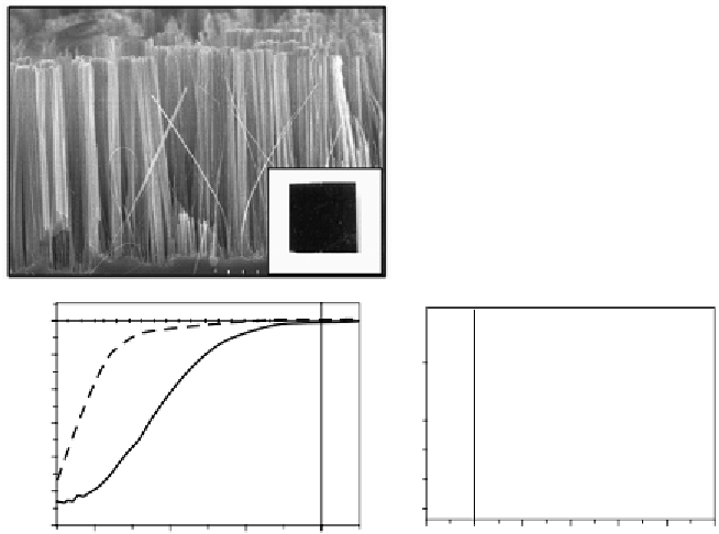
silicon for water reduction, Oh et al. reported to use
p
-type silicon nanowire
array photocathode fabricated via metal-catalyzed electroless etching
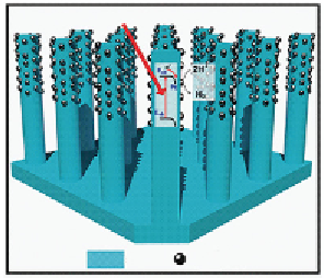
(Fig. 3.6a). The silicon nanowire arrays were further impregnated with Pt
nanoparticles (Fig. 3.6b). The nanowire-arrayed electrode significantly
Light
(a)
(b)
10µm
Platinum
Nanoparticle
Silicon
(c)
(d)
0
0
-5
-10
-10
-15
-20
-20
SINW (Light)
SINW (Dark)
Planar Si (Light)
-25
-30
-30
-0.1
0.0
0.1
0.2
0.3
0.4
0.5
-0.6
-0.4
-0.2
0.0
E (V vs. RHE)
E (V vs. RHE)
FIGURE 3.6
(a) SEM image of silicon nanowire arrays fabricated by metal-catalyzed chemical etching;
inset is the photograph of ∼10 mm × 10 mm silicon nanowire array sample with low reflection. (b)
Schematic of silicon nanowire arrayed photoelectrode. Photon absorbed by silicon nanowire generates
minority carrier, which drifts to semiconductor/electrolyte interface where H
+
is reduced to H
2
. Silicon
nanowires are impregnated with Pt nanoparticles that serve as electrocatalysts for water reduction.
(c) PEC performance of bare silicon nanowire and planar silicon film. (d) PEC performance of Pt modi-
fied planar silicon and nanowire silicon.
Source
: Reproduced with permission from Oh et al. [36]. (See
color insert.)


Search WWH ::

Custom Search