Environmental Engineering Reference
In-Depth Information
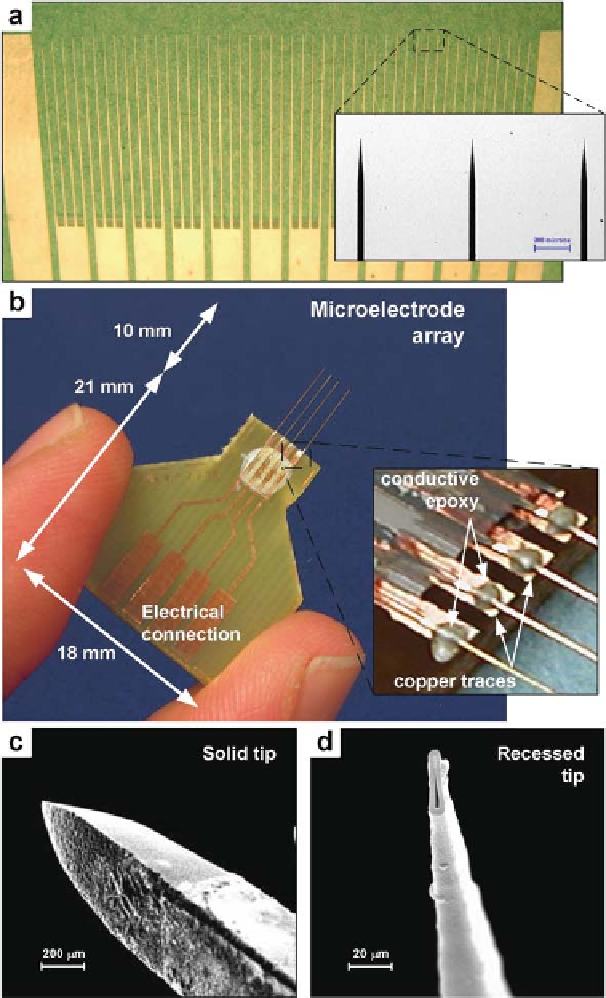
Fig. 6.6
Photographs of (
a
) an etched glass wafer with probe tips at the center and near the edges.
Close-up shows parallel tip ends at 900
m center-to-center spacing, and (
b
) the fabricated DO
microelectrode array sensor packaged on a PCB carrier. Close-up shows the design of the MEA
packaging using conductive silver epoxy. Scanning electron micrographs (SEMs) of (
c
) sharpened
solid tip, and (
d
) recessed tip at 45
◦
beveling angle. (Adapted from [57-59])
μ