Environmental Engineering Reference
In-Depth Information
is expected that the demonstrated multi-analyte MEA sensor will enable
in situ
measurements and analyses in environmental applications. Ultimately, these sen-
sors offer the ability to penetrate samples, due to the small tip size, for
in situ
measurements, as well as providing an array structure for higher robustness and
multi-analyte measurements.
6.2.2 MEA Fabrication
The needle-type MEA was fabricated from 175
50 mm borosilicate
glass wafers (Erie Scientific, Pittsburgh, PA). Batch fabrication was used to facilitate
fabrication of a large number of sensors, reduce costs, and increase yield. Twelve
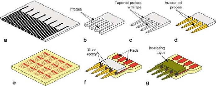
MEAs could be fabricated from a single glass wafer. The process, illustrated in
Fig. 6.3, has five major steps: dicing, etching, metallization, packaging, and sensor
tip formation.
Dicing.
Glass wafers were cleaned with sulfuric peroxide solution (H
2
SO
4
and
H
2
O
2
in a 7:3 (v/v) ratio) and cut with a dicing saw to yield an array of glass probes
(Fig. 6.3a). A 10 mil thick, 45
μ
m thick, 45
×
m diamond grit resinoid blade (K&S Micro-Swiss,
Fort Washington PA) was used to form 900
μ
m center-to-center spacing between
each glass probe, 2 cm in length. Alternatively, dicing can be outsourced (e.g.,
American Dicing Co., Syracuse, NY). Longer 2.5 cm cuts were made between every
four probes to define the edges of individual MEAs. In a later process step, an addi-
tional cut across the arrays would be made to separate individual MEAs. However,
keeping MEAs together at this time permits batch processing, increasing yield and
reducing fabrication costs. The cut wafer was then annealed at 550ºC for 10 min in
a programmable box furnace (Lindberg/Blue M, Thermo Scientific, Norwood, MA)
to relieve stress from the dicing process. Three cooling steps were used to reduce
thermal shock: 480ºC was reached at ~12ºC/min, followed by 24ºC/min cooling
μ
Fig. 6.3
Microelectrode array (MEA) sensor batch fabrication sequence: (
a
) dice glass wafer, (
b
)
form glass probes by dicing, (
c
) use meniscus etching to sharpen probes, (
d
) deposit Au conduc-
tive layer, (
e
) pattern PCB, (
f
) use silver epoxy to establish electrical connections, and (
g
)coat
microelectrodes with parylene insulating layer and fabricate recessed tips [55, 57]