Environmental Engineering Reference
In-Depth Information
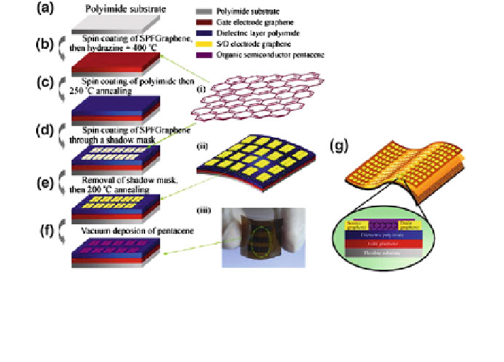
Fig. 4.8 (a-f) Schematic illustration of the fabrication of pentacene OFET devices. (i) Structure
of graphene; (ii) a schematic representation of the unfinished OFET before adding the pentacene
layer, showing its good flexibility; (iii) the finished pentacene OFET on a flexible PI substrate
when bent under force. (g) A schematic illustration of the structure of flexible bottom-contact
OFETs based on a pentacene film. Reproduced with permission [
54
]. Copyright 2011, Springer
is generally Al. Recently, Lee et al. reported a semitransparent inverted-type
polymer solar cell using a top laminated graphene electrode [
55
]. The device was
fabricated with a standard inverted structure using ZnO as electron transport layer,
replacing the PEDOT:PSS hole-transporting layer by GO and the top metal
electrode by the laminated CVD graphene film (Fig.
4.9
a). The detailed fabrica-
tion process was presented in Fig.
4.9
b. The resulting device structure was ITO/
ZnO/P3HT:PCBM/GO/graphene. As illuminated from the ITO side, the semi-
transparent device achieves a best PCE of 2.50 % when the top electrode with 10
layers of graphene was employed, corresponding to 76 % of that of the standard
opaque cell. The detailed performances were summarized in Table
4.3
. Similar
work has also been reported by Cox et al. using CVD graphene as back electrode
for small molecule OPV device [
56
]. These results indicate that besides employed
as window electrode in OPV, it can be used as back electrode. So, flexible, all-
carbon solar cells can be constructed using graphene as both anode and cathode.
4.4.3 All-Carbon Conductive Circuit
From solution-processing graphene films, we fabricated various graphene-based
microcosmic patterns and structures by computer controlled laser cutting
(Fig.
4.10
a-d, steps i-v) [
57
]. Furthermore, a complete working prototype of a
flexible
WORM
memory
card
coupled
with
a
real
data
retrieving
system
Search WWH ::

Custom Search