Environmental Engineering Reference
In-Depth Information
nitrogen and hydrogen, so that oxygen leaves the
film in the form of water vapor. The
resulting metallic alloy layer is transformed to the semiconductor alloy by gas
reaction at modest temperature with seleniumusing H
2
Se gas, producing the CIGS
absorber. Speaking approximately, this is a P-type semiconductor of controlled
bandgap and of thickness in the 1000 nm range. The thickness must be enough so
that most of the light is absorbed. Again, speaking approximately, the device is a PN
junction, and the next step, Junction formation, is accomplished by deposition of
CdS (CBD, or chemical bath deposition). The transparent electrode to the N-side of
the junction is ZnO (OMCVD, organometallic chemical vapor deposition). The
highest ef
ciency these workers achieved was 13.6% using a Mo-coated glass
substrate. A variation of this process that does not use Cd is described next.
This basic process is important because it uses the minimum amount of the
expensive metals, because it avoids expensive high vacuum equipment, and because
it can be scaled up to large areas. Think of printing a newspaper, how many square
meters of paper is printed by a major newspaper each day. The maximum efficiency
reported for this type of cell is nearly 20%. This value is close to the value 20.3%
mentioned for polycrystalline silicon cells, which are not amenable to a similar large-
scale nonvacuum fabrication. It appears that some form of this basic ink printing
process is employed in CIGSmanufacture by Nanosolar, Inc. in California, and ISET,
and for CdTe by a new
firm, Solexant.
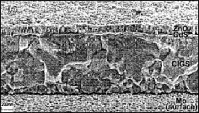
The cell shown in cross section in Figure 6.12 was formed on 12.5
m
m thick
commercial polyimide. TheMo back contact of 1
mwas deposited by DC sputtering.
The CIGS layer was established following sequential evaporation of the metals Cu,
In, and Ga, followed by evaporation of Se, with a controlled temperature anneal. The
CdS layer was then deposited in a chemical bath process. RF sputtering was used to
apply the upper window layer described as I-ZnO/ZnO:Al of 300 nm thickness.
Finally, Ni
-
Al contact grids for better current collection were applied by electron
m
Figure 6.12 Scanning electron microscope
cross-section image [76] of CIGS cell grown on
polyimide flexible substrate. Efficiency of 14.1%
was achieved in cells of this type. Layers, bottom
to top: polyimide (not shown), Mo back contact,
CIGS absorber layer, CdS junction-forming layer,
ZnO insulator layer, and ZnO:Al conductive
window layer.