Environmental Engineering Reference
In-Depth Information
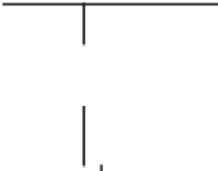
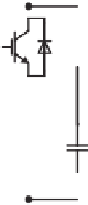
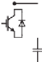
Figure 1.31
Lump snubber circuits.
Source:
FUJI 2004; POWEREX 2000
the capacitor, respectively. In practice,
V
is 0 and
V
equals the acceptable overshoot of the
voltage across the power switch and can be expressed as
V
=
k
m
V
CEm
−
V
d
,
where
V
CEm
is themaximumC-Ewithstood voltage of the power switch and
V
d
is the DC power
supply voltage, respectively. The coefficient
k
m
is less than 1, often 0.7-0.8 depending on the
particular IGBT, to make sure that the maximum voltage
V
d
+
V
is below the rated voltage.
The selection of the snubber resistance often depends on the reverse-recovery current of the
freewheeling diode and the minimum snubber resistance
R
s min
can be obtained empirically
(Hossain
et al
. 1997a) as
V
d
k
s
I
,
R
s min
=
where
k
s
,0
<
k
s
≤
0
.
2, is the reverse-recovery factor of the freewheeling diode.
1.3.2.5 Shoot-through of Phase Legs
Power switches cannot be turned ON or OFF instantaneously, although the process is very
fast. In order to avoid shoot-through between the upper and the lower switches of the same
phase leg, a short period of dead time is needed between the two gate signals. It can be set in
the controller, e.g. directly in a DSP or in a CPLD/FPGA chip. It can also be implemented with
deadtime generator ICs. For example, IXDP630/631 are able to inject the required deadtime to
convert a single-phase PWM signal into two separate logic signals required to drive the upper
and lower switches in a PWM inverter. It also provides functions for output disable, and fast
over-current and fault condition shutdown (IXYS 1998).
Although it is important to make sure that no shoot-through happens, it is also important to
note that excessive deadtime may deteriorate the performance, e.g. increased harmonics, etc.
It is also important for the deadtime to be applied symmetrically to the ON and OFF states to
minimise the DC component in the output voltage.


Search WWH ::

Custom Search