Environmental Engineering Reference
In-Depth Information
where the output impedance
Z
o
(
s
)is
sL
+
K
i
Z
o
(
s
)
=
K
R
(
s
)
.
1
+
When there is no load, the output voltage
v
b
is the same as the reference voltage
√
2
V
sin(
2
3
v
rb
=
ω
t
−
)
and, similarly, the output voltage
v
c
is the same as the reference voltage
√
2
V
sin(
2
3
v
rc
=
ω
t
+
)
.
There is not any phase shift or voltage drop.
If there is a load, then the voltage changes slightly because of the load effect. The smaller the
output impedance, the smaller the voltage change. In particular, this is true for the harmonic
voltage components. In order to improve the THD of the output voltage, the output impedance
at harmonic frequencies should be small. This can be done by selecting appropriate
K
R
(
s
).
If the real part of
K
R
(
s
) is positive, then the THD of the phase voltage can be reduced. The
block
K
R
(
s
) can be chosen to have high gains to obtain a small output impedance at harmonic
frequencies. There are many ways to design
K
R
. One of them is to use the resonant harmonic
compensator (Castilla
et al
. 2009; Shen
et al
. 2010)
2
ξ
h
ω
s
K
R
(
s
)
=
)
2
×
K
h
s
2
+
2
ξ
h
ω
s
+
(
h
w
h
=
3
,
5
,
···
of which the gain at frequency
h
w
is
K
h
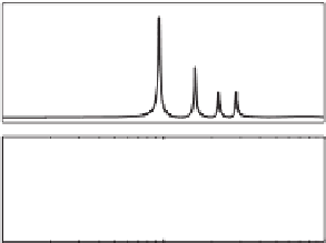
with zero phases; see e.g. the Bode plot shown in
Figure 14.7 for 1
01 that is to be used in simulations later. It is almost
1 everywhere apart from around the harmonic frequencies. This means the output impedance
can be tuned to be different values at different harmonic frequencies to improve the THD. For
most cases, the coefficients
K
h
should be between 1 and 20 with large values for low-order
harmonics and small values for high-order harmonics.
+
K
R
(
s
) with
ξ
=
0
.
24
1+K
3
20
16
1+K
1+K
7
12
8
1+K
9
4
0
90
45
0
−45
3ω
5
7ω 9ω
ω
−90
10
2
10
3
10
4
Frequency (rad/sec)
Figure 14.7
Bode plot of 1
+
K
R
(
s
) used in simulations


Search WWH ::

Custom Search