Environmental Engineering Reference
In-Depth Information
v
o
-
1
sL
i
e
−
Ts
s
K
i
-
u
v
r
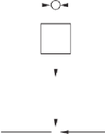
Figure 7.3
Approximate block diagram for the current loop
then the proportional gain is limited. The effect of computation and PWM conversion can be
approximated by a one-step delay
e
−
T
s
s
, where
T
s
is the sampling period. Then, an approximate
block diagram for the control loop is shown in Figure 7.3.
The characteristic equation of the loop is
K
i
sL
e
−
T
s
s
1
+
=
0
.
If the gain is chosen to satisfy
K
i
<
2
L
T
s
,
(7.2)
4
T
s
, the phase margin of the loop is
4
rad. Note that the
analysis done here is to demonstrate that there is a limit, sometime very strict, on the current
feedback gain. The gain
K
i
should be further decreased if a low-pass filter is involved in the
measurement of the current
i
.
π
L
then the loop is stable. When
K
i
=
7.3 Inverters with Capacitive Output Impedances (C-inverters)
The inductor current
i
can be measured to construct an integral controller
1
sC
o
,asshownin
Figure 7.4, so that the output impedance of the inverter is forced to be capacitive and that it
dominates the impedance between the inverter and the AC bus. This is equivalent to having a
virtual capacitor
C
o
connected in series with the filter inductor
L
, as will be shown later.
The following two equations hold for the closed-loop system consisting of Figure 7.1(b)
and Figure 7.4:
1
sC
o
u
=
v
r
−
i
and
u
f
=
sLi
+
v
o
.


Search WWH ::

Custom Search