Environmental Engineering Reference
In-Depth Information
its composing cells. Usually, voltages of 12 or 24 V are desired. A major advan-
tage of all thin film technologies is that the serial connection of the individual
cells to a module may be combined with the actual cell manufacturing. While the
process of serial connection is totally independent from the manufacturing of wa-
fer-based solar cells and is performed a posteriori, thin film modules consist of
lamellar arrangements of individual cells placed on a single substrate or super-
strate (Fig. 6.12).
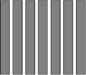
7 Cells
7 Cells
Glass superstrate
Glass superstrate
Rear contact
Rear contact
Absorber
Absorber
Front contact
Glass superstrate
Connection area
Front contact
Glass superstrate
Connection area
Fig. 6.12
Integrated serial connection of the cell strips of a thin film solar cell on the sub-
strate (i.e. the serial connection links the bottom electrode of a cell strip to the top electrode
of the next strip)
For the series connection of the cell strips, three structuring steps must be per-
formed during cell manufacturing. Fig. 6.13 illustrates the production principle of
such an integrated serial connection taking a hydrogen-passivated amorphous
silicon (a-Si:H) thin film solar cell as an example. Firstly, the glass superstrate is
coated with a conductive transparent layer of indium stannous oxide. What later
on will become the front contact, is removed with regular intervals during the first
structuring step. Structuring may either be performed by laser removal or by sim-
ple mechanical scraping off. Within the following preparation step, the photovol-
taically active layer ("absorber") is deposed. For a solar cell made of hydrogen-
passivated amorphous silicon (a-Si:H) this manufacturing step encompasses the
deposition of three layers (p-doped, i-doped and n-doped a-Si:H) in case of a sim-
ple p-i-n-type cell or a sequence of six layers for manufacturing of a tandem cell.
After the deposition of the absorber a second, a slightly parallel located structur-
ing step is performed, which removes the absorber layer but not the front contact.
Then the rear contact is deposited, so that by the two preceding structuring steps
the front contact of a cell strip is connected to the rear contact of the next strip.
Short-circuiting of individual cell strips by the rear contact is prevented by a third
structuring step. The approach is analogous for substrate-based technologies.


Search WWH ::

Custom Search