Civil Engineering Reference
In-Depth Information
nanoporosity, and then one should make use of low substrate temperatures
and high plasma gas pressures in order to reach 'zone 1'. Films of the latter
kind are required for a number of eco-effi cient technologies such as for
energy effi cient and comfort enhancing electrochromic 'switchable glazings'
in buildings, for gas sensors devised for air quality assessment, and for
photocatalytic surfaces capable of cleaning air and water (Granqvist,
1995; Smith and Granqvist, 2010); electrochromics is discussed further in
Chapter 11.
Multilayer fi lms are readily made by sequential evaporation or sputtering
from more than one source and a practical deposition unit can incorporate
a large number of sources which the substrate is transported past in a more
or less continuous process which we return to below for the case of sput-
tering. Composite fi lms can be prepared by deposition from one source of
a compound material (as long as decomposition of this material does not
take place) or from simultaneous deposition from two or more sources.
Mixed metal-dielectric fi lms can be deposited reactively, for example in the
presence of a small amount of oxygen, so that the deposit comprises a
random mixture of metallic and oxidized parts (known as a 'cermet' fi lm).
The underlying processes for reactive sputtering can be modelled very
accurately (Berg and Nyberg, 2005).
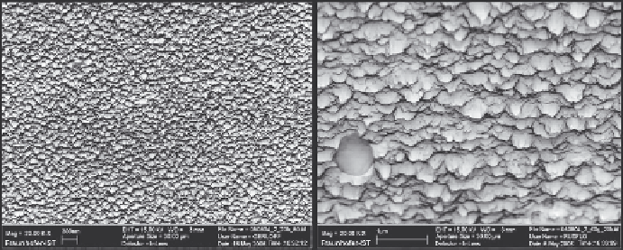
Chemical post-treatment of thin fi lms can modify the properties and lead
to novel properties. Figure 8.4 shows one example where a sputter depos-
ited fi lm of ZnO:Al - a transparent conductor - is roughened by etching in
dilute hydrochloric acid (Ruske
et al.
, 2007). The treated fi lm exhibits sig-
nifi cant light scattering. Chemical etching of some alloy fi lms can yield
highly nanoporous conducting layers (Maaroof
et al.
, 2005; Cortie
et al.
,
2006). An example is shown in Fig. 8.5, which reports on a sputter deposited
AuAl
2
fi lm after etching so that nothing but the gold remains.
(a)
(b)
8.4
Scanning electron micrographs of a sputter deposited ZnO:Al fi lm
(a) before and (b) after etching in 0.5% HCl. From Ruske
et al.
(2007).
Search WWH ::

Custom Search