Civil Engineering Reference
In-Depth Information
100 nm
100 nm
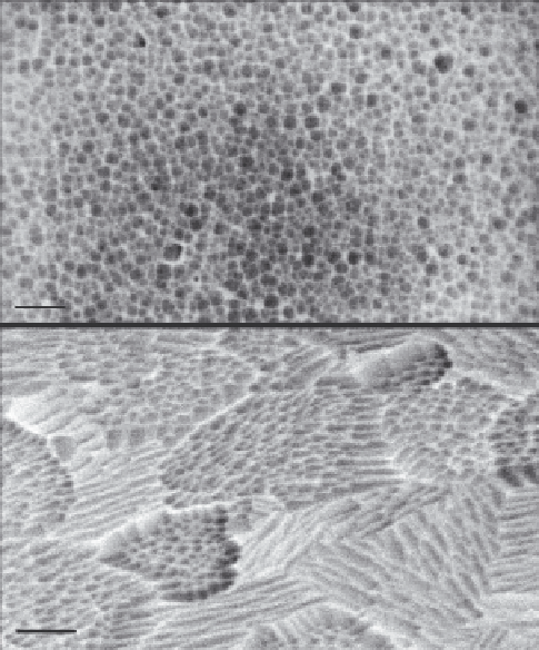
8.2
Scanning electron micrographs of an In
2
O
3
:Sn fi lm sputter
deposited at ambient temperature and annealing post-treated at 200°C
(top) and for an analogous fi lm sputter deposited onto a substrate
maintained at 200°C (bottom). From Betz
et al.
(2006).
The development of the structure depends critically on deposition and
post-treatment parameters, to an extent that might seem surprising. Thus,
for example, depositing a gold fi lm at room temperature and then heating
it to a certain temperature is not equivalent to direct deposition onto a
substrate at the same elevated temperature, as shown in a sequel to the
work from which Fig. 8.1 was reproduced (Lansåker
et al.
, 2012). Another
example of this sensitivity to the fi lm preparation conditions is shown in
Fig. 8.2 for the case of sputter deposited fi lms consisting of In
2
O
3
:Sn (Betz
et al.
, 2006), which is a transparent and electrically conducting material of
very large importance in energy technology and for transparent electronics
of different kinds. The top panel illustrates a scanning electron micrograph
for a fi lm deposited onto a substrate at room temperature and then anneal-
ing post-treated at 200°C and the bottom panel pertains to a fi lm that was
sputtered onto a substrate at 200°C. Clearly the two fi lms display striking
differences.
Search WWH ::

Custom Search