Civil Engineering Reference
In-Depth Information
The plasma is normally confi ned to the target area by magnets placed
behind the target, and one then refers to the deposition technique as 'mag-
netron sputtering'. Rotating targets can be used for maximum utilization of
the deposition material. The deposition species typically have energies of
some electron volts, i.e., the energies are higher than in the case of evapora-
tion and are large enough to remove contaminants from the substrate. This
self-cleaning feature is conducive to a good adherence between substrate
and fi lm, which is an advantage for sputtering when compared with evapo-
ration as a thin fi lm technology.
Evaporation and sputtering are often referred to jointly as 'physical
vapour deposition' or PVD. What do thin fi lms made by these techniques
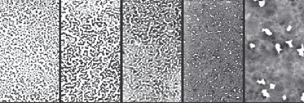
look like at the nano level? We consider the growth of metal fi lms on
dielectric substrates, such as glass or polymer. Figure 8.1 illustrates a series
of scanning electron micrographs taken on gold fi lms with the shown
thicknesses and deposited by sputtering onto glass at room temperature
(Lansåker
et al.
, 2009). The initial deposition is seen to yield tiny metallic
nuclei at certain sites on the substrate, and continued deposition makes
these nuclei grow, which is expected to occur via diffusion of atoms or
molecules over the substrate surface as well as by direct impingement of
atoms or molecules. The discrete metal 'islands' that are then formed have
shapes that somewhat resemble ellipsoids. Continued deposition makes
some of the 'islands' touch and rearrange into larger and more irregular
objects; this is conventionally referred to as 'coalescence growth'. The
growing fi lm then passes through what can be called 'large-scale coales-
cence', meaning that a contiguous and meandering metallic network of
macroscopic extent is formed. Only then can metallic conduction be
detected along the fi lm. The evolution of electromagnetic properties in a
growing metal fi lm is a topic of continued interest and is highly dependent
on the prevailing nanostructures (Earp and Smith, 2011).
t
eq
(nm):
2.6
4.4
6.2
8.0
9.8
200 nm
8.1
Scanning electron micrographs of gold fi lms made by sputtering
onto glass to the shown equivalent thickness
t
eq
(i.e., the thickness a
corresponding metallic slab would have). The gold appears bright and
the uncoated parts of the substrate look dark. From Lansåker
et al.
(2009).


Search WWH ::

Custom Search