Environmental Engineering Reference
In-Depth Information
estimated to be more than 50 $/kAm, which may be acceptable in niche rotating
machine markets, but too expensive for the wind market.
5.2 2G HTS wire technology
The new 2G wires are based on the superconducting material YBa
2
Cu
3
O
x
nor-
mally referred to as YBCO-123 or simply YBCO. The structure and manufactur-
ing method of 2G HTS wire is very different form that of 1G wire. YBCO was
one of the fi rst HTS materials to be discovered and is easily made in bulk form
by growing a crystal in a similar manner to silicon. Development of YBCO-based
wire began in the 1990s by attempting to deposit a crystal of YBCO onto a metal
substrate tape. This technique has now been extensively developed by several
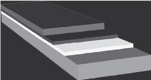
manufacturers using a number of different processes. The wire structure consist
of a substrate, typically a Nickel-Tungsten alloy, a very thin buffer layer onto
which is deposited the YBCO superconductor to a thickness of 1-5 µm. Often an
outer copper layer is added for stability. The overall wire thickness is between 0.1
and 0.2 mm thick depending on the manufacturer and product. The coatings are
deposited on a wide strip of the substrate and then slit to the required tape width.
This gives fl exibility in the fi nal width and current carrying capacity of the HTS
tape, the most common being 4 mm for compatibility with 1G HTS materials, and
12 mm for higher current carrying capacity. A simplifi ed wire structure is shown in
Fig. 5, some processes introduce additional buffer layers. It is also possible to join
two of these tapes back to back to produce a symmetrical duplex tape.
This type of HTS wire has the potential for volume production at low cost. It
does not require the large fl oor space the 1G wire need for the drawing process,
since the 2G process can be reel to reel, and once the correct process parameters
are set up production remains almost entirely automated.
HTS materials are intrinsically anisotropic, and their sensitivity to magnetic fi eld
depends on the direction of the fi eld relative to the surfaces of the HTS tape. It has
been necessary to develop methods in the manufacturing process that minimise the
effect of this anisotropic behaviour [32].
Copper
HTS
Buffer
Substrate
Figure 5: Simplifi ed 2G wire structure - thickness scale exaggerated.


Search WWH ::

Custom Search