Hardware Reference
In-Depth Information
-75 = 7.5ns @ CL2 latency (DDR 266)
The full datasheet for this example is located at
From this information, you can determine that the module has the following characteristics:
• The module runs at DDR266 speeds using standard 2.5V DC voltage.
• The module has a latency of CL2, so you can use it on any system that requires CL2 or slower
latency (such as CL2.5 or CL3).
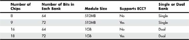
• Each chip has a capacity of 512Mb (64 × 8 = 512).
• Each chip contains 8 bits. Because it takes 8 bits to make 1 byte, you can calculate the capacity
of the module by grouping the memory chips on the module into groups of eight. If each chip
contains 512Mb, a group of eight means that the module has a size of 512MB (512Mb × 8 =
512MB). A dual-bank module has two groups of eight chips for a capacity of 1GB (512Mb × 8
= 1024MB, or 1GB).
If the module has nine instead of eight memory chips (or 18 instead of 16), the additional chips are
used for parity checking and support ECC error correction on servers with this feature.
To determine the size of the module in megabytes or gigabytes and to determine whether the module
supports ECC, count the memory chips on the module and compare them to
Table 6.13
. Note that the
size of each memory chip in megabits is the same as the size in megabytes if the memory chips use an
8-bit design.
Table 6.13. Module Capacity Using 512Mb (64Mbit × 8) Chips
The additional chip that each group of eight chips uses provides parity checking, which the ECC
function employs on most server motherboards to correct single-bit errors.
A registered module contains 9 or 18 memory chips for ECC plus additional memory buffer chips.
These chips are usually smaller in size and located near the center of the module, as shown
previously in
Figure 6.10
.
Note
Some modules use 16-bit wide memory chips. In such cases, only four chips are needed for
single-bank memory (five with parity/ECC support), and eight are needed for double-bank
memory (10 with parity/ECC support). These memory chips use a design listed as capacity
times 16, like this: 256Mb × 16.
You can also see this information if you look up the manufacturer and the memory type in a search
engine. For example, a web search for
Micron Unbuffered DIMM Design
locates a table showing
various DIMM organization, SDRAM density, and other information for listed modules.