Hardware Reference
In-Depth Information
In 2002, chip manufacturing began moving from 200mm (8-inch) diameter wafers to larger 300mm
(12-inch) wafers. The larger 300mm wafers enable more than double the number of chips to be made
compared to the 200mm used previously. In addition, the transitions to smaller and smaller processes
enable more transistors to be incorporated into the chip die.
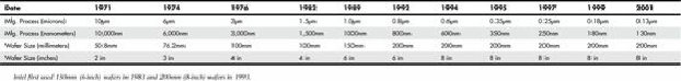
Table 3.8
shows the CPU manufacturing process and silicon wafer size transitions for the first 30
years from when the processor debuted (1971-2001).
Table 3.9
shows the continuing evolution of
these transitions from 2002 through the present, and all the way to 2022, including several planned
future transitions.
Table 3.8. CPU Process/Wafer Size Transitions from 1971 to 2001
Table 3.9. CPU Process/Wafer Size Transitions from 2002 to 2022
With more recent processors, smaller manufacturing processes have also been used to make more
space available in each processor die for features such as multiple processor cores, CPU-integrated
video, and large L3 caches. Thus, the Nehalem Core i7 six-core processor, although it uses a 45nm
process, has a much larger core size than the Pentium 4 Northwood (which was built on a 130nm
process): 263 square millimeters for the Nehalem (731 million transistors), versus just 131 square
millimeters for Northwood (55 million transistors). As a result, the Nehalem Core i7 processors have
a yield of 240 die candidates per wafer, about half of the yield of the Northwood.
These will still be made on 300mm wafers because the next wafer transition isn't expected until
2014, when a transition to 450mm wafers is expected.
Note that not all the chips on each wafer will be good, especially as a new production line starts. As
the manufacturing process for a given chip or production line is perfected, more and more of the chips
will be good. The ratio of good to bad chips on a wafer is called the
yield
. Yields well below 50%
are common when a new chip starts production; however, by the end of a given chip's life, the yields
are normally in the 90% range. Most chip manufacturers guard their yield figures and are secretive
about them because knowledge of yield problems can give their competitors an edge. A low yield
causes problems both in the cost per chip and in delivery delays to their customers. If a company has
specific knowledge of competitors' improving yields, it can set prices or schedule production to get
higher market share at a critical point.
After a wafer is complete, a special fixture tests each of the chips on the wafer and marks the bad
ones to be separated later. The chips are then cut from the wafer using either a high-powered laser or
a diamond saw.
After being cut from the wafers, the individual dies are retested, packaged, and retested again. The
packaging process is also referred to as
bonding
because the die is placed into a chip housing in
which a special machine bonds fine gold wires between the die and the pins on the chip. The package