Hardware Reference
In-Depth Information
each chip are built one on top of the other until the chips are completed (see
Figure 3.7
).
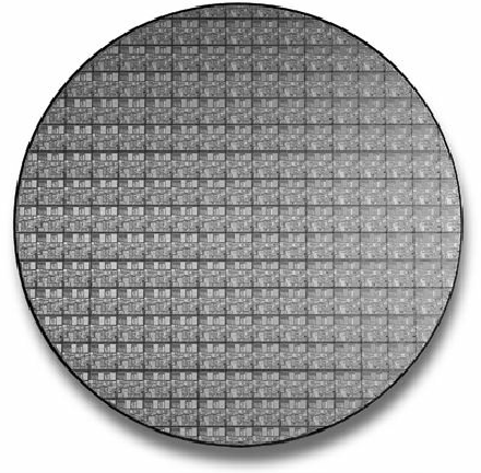
Figure 3.7. 200mm (8-inch) wafer containing 177 full Pentium 4 Northwood (0.13-micron)
processor cores.
Some of the masks add the
metallization
layers, which are the metal interconnects that tie all the
individual transistors and other components together. Most older chips use aluminum interconnects,
although in 2002 many moved to copper. The first commercial PC processor chip to use copper was
the 0.18-micron Athlon made in AMD's Dresden fab, and Intel shifted the Pentium 4 to copper with
the 0.13-micron Northwood version. Copper is a better conductor than aluminum and allows smaller
interconnects with less resistance, meaning smaller and faster chips can be made. Copper hadn't been
used previously because there were difficult corrosion problems to overcome during the
manufacturing process that were not as much of a problem with aluminum.
Another technology used in chip manufacturing is called silicon on insulator (SOI). SOI uses a
layered silicon-insulator-silicon wafer substrate to reduce parasitic device capacitance, thus reducing
current leakage and improving performance. In particular, AMD has used SOI for many of its
processors since 2001.
A completed circular wafer has as many chips imprinted on it as can possibly fit. Because each chip
usually is square or rectangular, there are some unused portions at the edges of the wafer, but every
attempt is made to use every square millimeter of surface.
The industry is going through several transitions in chip manufacturing. The trend in the industry is to
use both larger wafers and a smaller manufacturing process. The
process
refers to the size and line
spacing of the individual circuits and transistors on the chip, whereas the
wafer size
refers to the
diameter of the circular wafers on which the chips are imprinted.
The industry began moving to the 90-nanometer (0.09-micron) process in 2004, the 65-nanometer in
2006, the 45-nanometer process in 2008, the 32-nanometer process in 2010, and the 22-nanometer
process in 2012.